2nm Chips Explained: GAA Nanosheet and Backside Power
2nm Chips Explained: GAA Nanosheet Transistors and Backside Power Delivery
I almost skipped the “2nm” headlines the way I skip a software update prompt at 11pm. Then I noticed the same two words sitting under three things I actually pay for: the next iPhone, my laptop, and my monthly AI bill. So I went looking for a plain-English answer to 2nm chips explained: GAA nanosheet transistors and backside power delivery — and found a wall of engineer-grade physics on one side and stock-tip hot takes on the other.
Neither answered my question: do I need to care, and what does this change for the stuff I use every day?
Here’s the honest version. I’ll argue both sides — that 2nm is a real generational leap, and that it’s a marketing rebrand — then tell you where I landed, what I got embarrassingly wrong, and how it connects to the cost of running AI.
What a 2nm chip actually is (and isn’t)
Let me kill the biggest myth first, because I believed it for years.
The “2nm” label is a process-node name, not a measurement. Nothing inside the chip is 2 nanometers wide. It’s a marketing label foundries use to mark a new generation of manufacturing — the way a car model year doesn’t tell you the engine displacement. The actual transistor features are larger; the number is a brand, not a ruler.
That single fact reframes the whole debate. Once you stop reading “2nm” as a width, you can ask the better question: what genuinely changed in this generation, versus what’s just a new sticker?
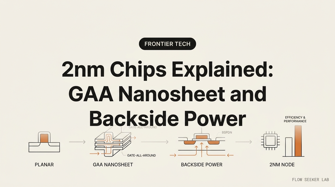
Two things changed at once, and that’s why this round matters more than the last few.
The first is the transistor shape — the industry moved from FinFET to gate-all-around (GAA) nanosheet transistors. The second is where the power wiring runs — a new approach called backside power delivery. I’ll take each side of the “is it a real leap” argument using these two as the evidence.
Side A: this is a genuine generational leap
Start with the case for “yes, this is the real thing.”
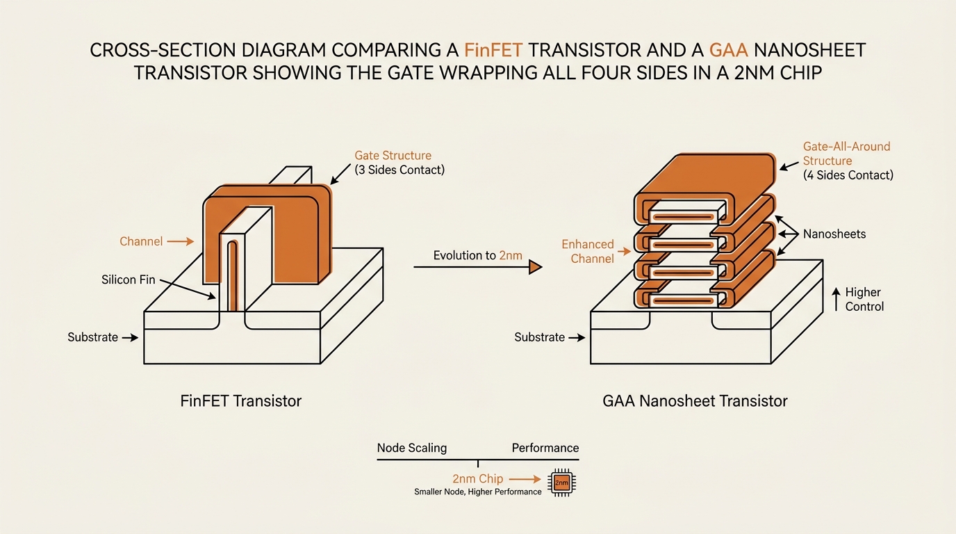
For about a decade, every advanced chip used a FinFET — a transistor where the gate (the on/off switch) wraps around three sides of a thin vertical “fin.” FinFET arrived around 2011 and carried the industry through node after node. But below roughly 7nm-class gate lengths, it starts leaking. The gate loses fine control over the current, an effect engineers call short-channel leakage. You can shrink the label, but the physics stops cooperating.
GAA nanosheet transistors fix that by wrapping the gate around all four sides of stacked horizontal sheets of silicon. More contact means tighter control, less leakage, and the ability to tune each transistor by widening or stacking the sheets. The Synopsys explainer on gate-all-around transistors lays out the electrostatics if you want the deep version. For our purposes, the headline is simple: this is the first transistor-architecture change since FinFET. Not a shrink. A new structure.
Then there’s backside power delivery, which is the part that made me sit up.
In a normal chip, the power wires and the data-signal wires both run on the front of the silicon, on top of the transistors. As features got denser, those two traffic systems started fighting for space, and power had to squeeze through a long, congested path — causing voltage to sag. Backside power delivery moves the power wiring to the back of the wafer, leaving the front free for signals. Cleaner power, less congestion, better efficiency. The Wikipedia entry on gate-all-around FETs is a neutral starting point if you want a vendor-free overview.
Put GAA and backside power together and the case for “generational leap” is strong. New transistor shape, new power architecture, two structural changes landing in the same generation. This is the engineering that keeps Moore’s Law breathing for another few years instead of flatlining. On the silicon, Side A is correct.
Side B: it’s an incremental rebrand
Now the uncomfortable counter-case, because it’s also true.
Start with the name. “2nm” isn’t 2 nanometers of anything, and the gap between the label and the reality has never been wider. A buyer who hears “2nm” pictures something twice as small and twice as good as “4nm.” The actual user-facing improvement is far more modest.
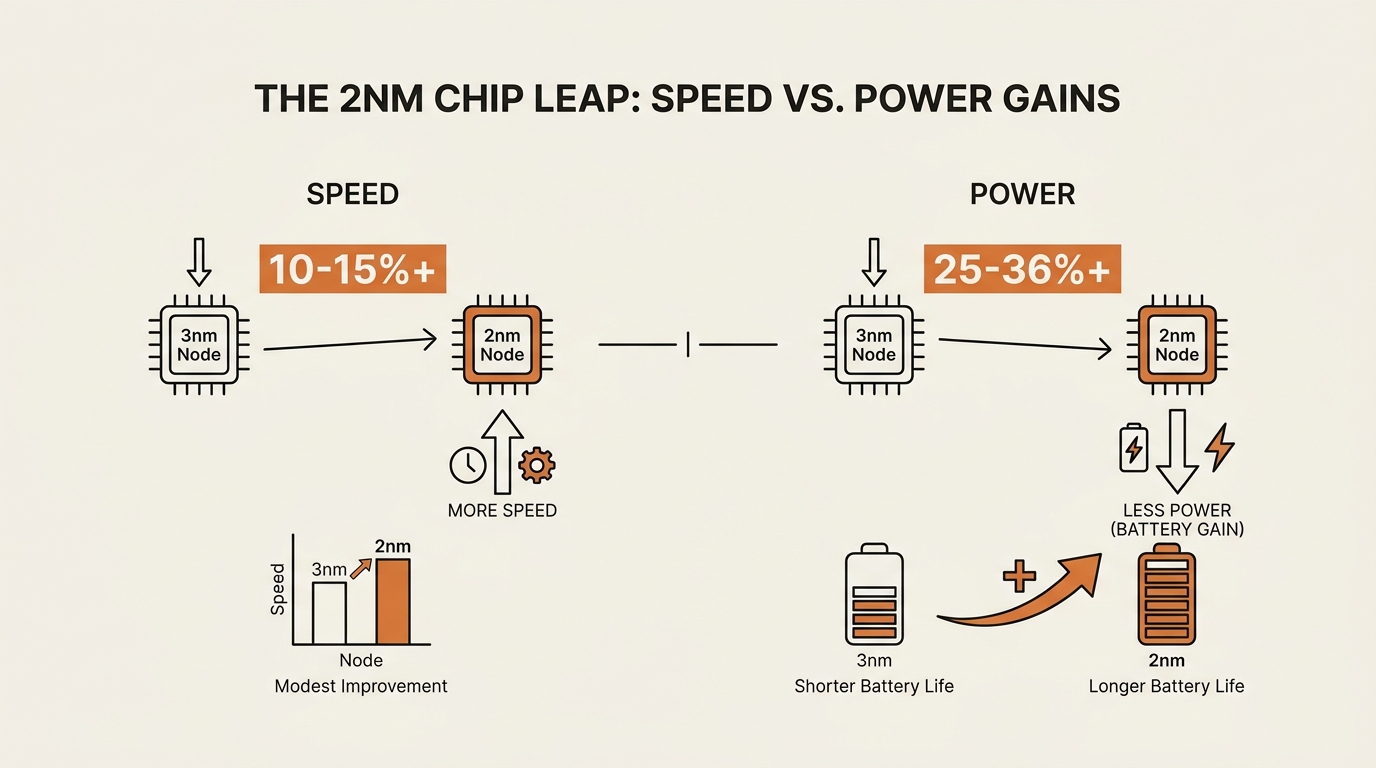
Here are the numbers I trust. Versus the previous 3nm generation, a 2nm chip delivers roughly 10–15% more performance at the same power, or about 25–36% less power at the same performance. That’s the real spread foundries quote. Tom’s Hardware reported TSMC’s first 2nm node at up to 15% improvement at iso-power when it began volume production.
Read those numbers as a normal person, not an engineer. A 10–15% speed bump is not something you’ll feel scrolling Instagram. Your apps already open instantly. What you might notice is the other half of the trade: better battery life, or a laptop that runs cooler and quieter. That’s nice. It is not a step-change. It is the same incremental gain every node has delivered for years, wearing a flashier number.
There’s a marketing wrinkle too. The “2nm” generation got split into sub-variants and staggered features, so what ships first may not include every advertised benefit. Backside power delivery, the part I found most exciting in Side A, isn’t even arriving uniformly across every 2nm-labeled product (more on that in the table below). So when a phone ad waves “2nm” at you, treat it like a model year. Something improved. The number is not a promise about your experience.
Side B’s verdict: for the person holding the phone, this is incremental. The leap is real in the fab, not in your hand.
Who makes 2nm chips, and who shipped what first
Both sides lean on specifics, so here’s the part the headlines blur together. Three foundries are racing on 2nm-class nodes, and they did not arrive with the same features. This is where the “generational leap” claim gets a useful asterisk.
The clean way to see it: GAA showed up everywhere this generation, but backside power delivery did not arrive at the same time as GAA. That mismatch is the single most misreported fact in 2nm coverage.
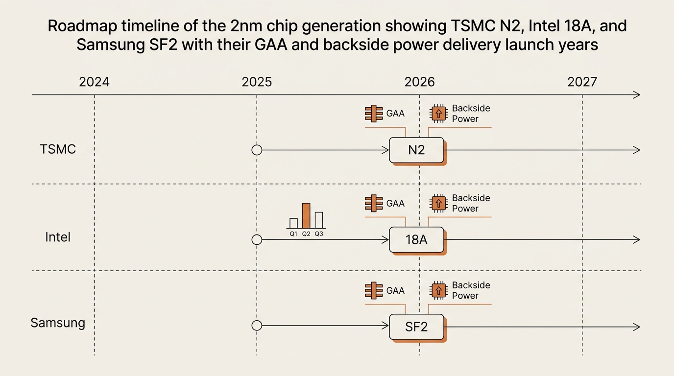
| Foundry node | GAA transistor | Backside power delivery | Volume production | First/notable products |
|---|---|---|---|---|
| TSMC N2 | Yes (TSMC’s first GAA node) | No — arrives later on TSMC A16 (“Super Power Rail”) | Late 2025 | Apple A20 / A20 Pro (iPhone 18 lineup), M6, Vision Pro R2 |
| Intel 18A | Yes (RibbonFET) | Yes (PowerVia) — first node anywhere to ship both together | Late 2025 | Intel “2nm-class” products |
| Samsung SF2 | Yes | No — comes later on SF2Z | ~Mid 2025 | Samsung 2nm products |
A few things this table makes obvious.
Intel 18A is the one that actually combined GAA and backside power delivery first in high-volume manufacturing — its GAA is branded RibbonFET, its backside power is branded PowerVia. Intel’s own 18A process page is the first-party source for that pairing. So when someone says “2nm finally brings backside power,” they’re describing Intel 18A — not TSMC’s first 2nm node.
TSMC N2 is GAA-only at launch. It’s TSMC’s first gate-all-around node, but backside power delivery moved to a later node, A16, whose mass production has widely been reported as slipping toward 2027. That’s an honest caveat worth holding: the full “generational leap” package, on TSMC’s roadmap, isn’t all in the first 2nm product.
Samsung SF2 entered production earlier but has faced yield challenges, with backside power coming later on SF2Z.
If you only remember one line from this section: GAA is the part that’s everywhere now; backside power delivery is staggered. Side A is right that both are real — but Side B is right that they don’t all land in your first 2nm device at once.
Where I was wrong about 2nm chips
This is the part the engineer blogs and the stock blogs both skip, so it’s the part I can actually add.
I thought “2nm” meant something inside the chip was 2 nanometers wide. It doesn’t. I’d been reading node names as physical measurements my whole life, picturing each generation as literally half the size of the last. That mental model is wrong, and it made every spec sheet feel more dramatic than it was. Once I learned the number is a brand, the marketing lost its grip on me — in a good way.
I assumed a node jump meant my next phone would feel dramatically faster. I expected the 3nm-to-2nm leap to be the kind of upgrade you notice in the first ten minutes. Then I read the real spread — 10–15% performance or 25–36% power — and realized I’d been pattern-matching “new transistor architecture” onto “huge speed boost.” Those aren’t the same thing. The architecture change is huge for the fab. The speed change for me is small. Holding both facts at once was the unlock.
I conflated GAA and backside power as one feature that ships together. Reading the headlines, I lumped “2nm = GAA + backside power” into a single bundle. The table above is the correction I needed: GAA is broad, backside power is staggered, and the foundry that shipped both first wasn’t the one I’d assumed. I had the vendor names tangled too — RibbonFET, PowerVia, Super Power Rail all blurred until I wrote them down side by side.
The boring truth: the technology is more impressive and less life-changing than the headlines made me feel. Both at once. That tension is the whole story.
What 2nm chips actually change for what you pay for
So where does a non-engineer land? Here’s my verdict, and it’s the same answer to the “leap or rebrand” question: both sides are right, because they’re measuring different things.
The engineering is a genuine generational leap. GAA nanosheet transistors plus backside power delivery is the most significant structural change to chips in over a decade. That part is not hype.
The experience in your hand is incremental. Your next phone will be a bit faster or last a bit longer, not transformed. That part is not hype either.
But there’s a third thing, and it’s the one that made me care: AI cost. This is the bridge no semiconductor explainer bothers to build for people like us.
Running a large AI model is mostly an energy and efficiency problem. Every ChatGPT or Gemini answer is a burst of computation, and the cost of that computation is tied to performance-per-watt — how much work a chip does per unit of power. Smaller, more efficient nodes like 2nm push performance-per-watt up. More efficient inference is part of why the price of running these models keeps drifting down, and it’s the same trend behind on-device AI — features that run on your phone instead of a far-off server. If you want the other half of that equation, I wrote about what a new flagship model launch actually changes for working professionals, and the same efficiency logic shows up in the open-source AI tooling I keep coming back to.
So the practical translation of this whole generation for a working professional is roughly this:
- Your phone: marginally faster, meaningfully better battery — not a reason to upgrade by itself.
- Your laptop: cooler, quieter, longer-lasting — efficiency over raw speed.
- Your AI bill: efficient nodes are one input keeping inference cheaper over time, which compounds as more AI moves on-device.
- The hype: a generational leap in the fab, an incremental bump in your hand — and “2nm” is a brand, not a width.
That’s the same “is the hype real?” filter I used on whether humanoid robots are actually going mainstream. The frame travels: separate the engineering reality from the experience reality, and the marketing stops steering you.
FAQ
What is a 2nm chip, and is it actually 2 nanometers? No. The label is a process-node name — a marketing tag for a new manufacturing generation — not a physical measurement. Nothing inside the chip is literally 2 nanometers wide. The actual transistor features are larger; the number marks a generation, the way a model year marks a car.
What’s the difference between GAA and FinFET transistors? A FinFET wraps the gate around three sides of a vertical fin. A gate-all-around (GAA) nanosheet transistor wraps the gate around all four sides of stacked horizontal sheets. More gate contact means tighter control and less leakage, which is why GAA replaces FinFET as features shrink below roughly 7nm-class gate lengths.
What is backside power delivery, and why does it matter? Backside power delivery moves the power wiring from the front of the chip to the back, separating it from the data-signal wiring. That eases congestion and reduces voltage sag, improving efficiency. It’s a structural change to how chips are wired, and it arrives on a staggered timeline rather than alongside every 2nm node.
Will a 2nm chip make my phone or laptop noticeably faster? Realistically, no big jump. Versus 3nm, expect roughly 10–15% more performance at the same power, or about 25–36% less power at the same performance. You’ll feel that mostly as better battery life and cooler running, not as a dramatic speed increase you notice while using apps.
Who makes 2nm chips — TSMC, Intel, or Samsung? All three. TSMC’s node is N2 (its first GAA node, GAA-only at launch). Intel’s is 18A, the first to ship GAA plus backside power delivery together. Samsung’s is SF2. They share the “2nm-class” label but differ on which features arrived first.
Which devices use 2nm chips first? The first mainstream consumer 2nm chips are Apple’s A20 and A20 Pro, built on TSMC N2, for the iPhone 18 lineup, alongside the M6 and Vision Pro R2. Intel’s 18A powers its own 2nm-class products. Apple reportedly took a large share of TSMC’s initial 2nm capacity.
Is the 3nm-to-2nm jump a real leap or just a rebrand? Both, depending on what you measure. The engineering — GAA nanosheet transistors plus backside power delivery — is a genuine generational leap, the biggest structural change in over a decade. The user-facing gain is incremental: a modest speed or battery improvement. The “2nm” name is a brand, not a width.
The frame I’m keeping
Here’s what changed for me. I stopped asking “is 2nm a big deal?” as a yes-or-no question, because the answer depends entirely on whether you’re standing in the fab or holding the phone. Split the question, and both answers snap into focus: real leap in the silicon, small bump in your pocket, and a quiet tailwind on the cost of running AI.
Next in this Framework Deep Dive series, I want to take the same “engineering reality versus experience reality” filter to on-device AI — the features that run on your phone instead of a server, and whether the privacy-and-speed pitch holds up once you actually use them.
seonjae — Korean office worker documenting his transition into AI systems, agents, and vibe coding — without a CS background. Shipping in public.